
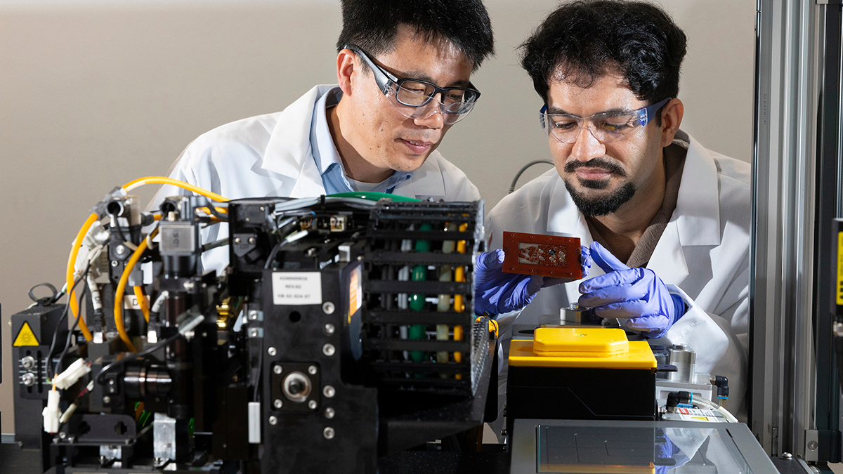
Associate professor Bayaner Arigong, Ph.D., (left) and doctoral student Saeed Zolfaghary Pour work in the Dragonfly IV Nanodimension 3d printer at the FAMU-FSU College of Engineering in Tallahassee, Florida. (Scott Holstein/FAMU-FSU College of Engineering)
Key points
- Researchers at Florida A&M University and the FAMU-FSU College of Engineering in Tallahassee, Florida, have developed a new AI-driven method for designing and fabricating microwave circuits using 3D printing.
- The team, led by Associate Professor Bayaner Arigong, Ph.D., of the Department of Electrical and Computer Engineering, used a computational technique called inverse design to automatically determine the optimal physical structure of a microwave power splitter—a core component in wireless communications and sensing systems.
- Their approach removes the need to begin with a fixed circuit layout, making it far easier to scale designs for different frequencies, devices and applications.
- The research was published in Communications Engineering, part of the Nature Portfolio journal family, and was supported by the Air Force Office of Scientific Research and the National Science Foundation.
A research team Florida A&M University and the FAMU-FSU College of Engineering has developed a new way to design and build microwave circuits—the high-frequency electronic components that underpin wireless communications, radar and sensing systems—using artificial intelligence and 3D printing.
Their work introduces a design method that lets a computer determine the best physical shape for a circuit, rather than requiring engineers to start from a predetermined blueprint. The result is a faster, more flexible path to building the kinds of electronic components that power everything from cellphone networks to advanced radar.
The study, “Inverse design and 3D printing of a multiport microwave power splitter: a scalable electromagnetic design framework,” was published in Communications Engineering, part of the Nature Portfolio journal family.

What Problem Were the Researchers Trying to Solve?
Traditional microwave circuit design relies on fixed layouts. Engineers start with a known circuit shape and work forward from there. That approach works for simple, well-established designs, but it becomes a serious obstacle when a system requires many signal ports, unusual geometries or rapid adaptation to new specifications.
Associate Professor Bayaner Arigong, of the Department of Electrical and Computer Engineering, leads the research group. Doctoral candidate Saeed Zolfaghary Pour is the study’s lead author. Both are associated with the joint college and Florida A&M University.
“Unlike conventional forward design and fabrication, our approach uses AI-driven inverse design without a predetermined circuit topology. By simultaneously 3D printing conductor and dielectric materials, we break through the limitations of traditional design to realize multifunctional microelectronics devices and circuits in true 3D form,” said Arigong.
How Does AI-Driven Inverse Design Work?
Instead of starting with a shape and calculating how it performs, inverse design works in reverse: engineers specify what they need the device to do, and an algorithm figures out what shape will do it best.
The team’s method uses a computational technique, a form of gradient-based optimization called adjoint electromagnetic simulation, to automatically sculpt the internal structure of a dielectric (electrically insulating) material until it meets precise performance targets across multiple output ports.
“Instead of starting with a fixed design, we tell the computer what we want the device to do, and it figures out the best structure,” said Zolfaghary Pour. “That opens up possibilities that are very hard to achieve with traditional methods.”
Because the final design comes directly from the optimization algorithm, not from a human-drawn schematic, the approach is what engineers call “topology-agnostic.” It is not constrained to any particular circuit shape. It is also “fabrication-aware,” meaning the algorithm accounts for the realities of manufacturing as it works.
Why Does 3D Printing Matter Here?
Once the algorithm produces an optimized design, the team fabricates it using multi-jet fusion (MJF), a form of polymer powder bed fusion 3D printing. The process builds up the device layer by layer, depositing both conducting and dielectric materials simultaneously to create a true three-dimensional structure—something conventional circuit manufacturing, which works mostly in flat layers, cannot easily achieve.
This direct compatibility with 3D printing means the team can go from a finalized design to a physical prototype quickly, without the expensive tooling and setup costs typically associated with custom electronic components.
To demonstrate the method, the researchers designed and built a four-port microwave power splitter operating at 10 GHz. Both computational simulations and physical measurements confirmed the device performed as intended, validating that the technique holds up in practice.

What Are the Key Advantages of This Approach?
The new design framework offers several capabilities that distinguish it from conventional methods.
- Rapid prototyping. 3D printing removes the need for masks or molds, cutting manufacturing lead time and up-front tooling costs.
- Design scalability. The same framework can be extended to devices with more ports, more complex 3D geometries and multiple simultaneous functions, without starting the design process over.
- Performance robustness. Devices designed using the inverse method maintain strong performance even with small variations in manufacturing—a key requirement for real-world deployment.
- Broad frequency range. The method can be applied across a wide spectrum, from direct current (DC) through radio frequency (RF) and into terahertz (THz) ranges.
What Applications Could Benefit From This Research?
The research has direct relevance for any system that relies on high-frequency electronic components. That includes telecommunications infrastructure—including next-generation 5G networks, as well as radar sensing, satellite communications and quantum communication systems.
One category of particular interest is beamforming phased arrays, which are antenna systems used in advanced radar and wireless communications to steer signals electronically. These systems require many signal-splitting components that must work in precise coordination, making scalable, flexible design methods especially valuable.
“This approach will bring new design methods to microelectronic circuits in many ways for communication, sensing and computing,” Arigong said.
Who Conducted the Research and Who Funded It?
The full research team includes Zolfaghary Pour as lead author; Hanxiang Zhang, a postdoctoral scholar; Po Wei Liu, a doctoral candidate; and Arigong, the principal investigator. All are affiliated with the Department of Electrical and Computer Engineering at the FAMU-FSU College of Engineering.
The research was supported by the Air Force Office of Scientific Research (grant FA9550-22-1-0028) and the National Science Foundation (grants EES-2428790 and EES-2230248).
Frequently Asked Questions
What is inverse design in electrical engineering? Inverse design is a computational approach in which an engineer specifies the desired performance of a device—such as how it should split a signal across multiple outputs—and an algorithm works backward to determine the physical structure that will achieve those results. This contrasts with conventional “forward” design, where engineers begin with a known circuit layout and calculate its expected behavior. Inverse design can find solutions that would be difficult or impossible to reach through traditional methods.
What is a microwave power splitter and why does it matter? A microwave power splitter is a passive electronic component that divides a high-frequency signal into two or more outputs. These devices are foundational to radar systems, wireless communications networks, satellite links and antenna arrays. In modern telecommunications—including 5G infrastructure and advanced sensing systems—power splitters must handle many signal paths simultaneously, making scalable, flexible designs increasingly important.
How does 3D printing improve microwave circuit manufacturing? Traditional circuit manufacturing works largely in flat, two-dimensional layers, which limits how complex a circuit’s physical geometry can be. 3D printing—specifically the multi-jet fusion (MJF) process used in this study—can deposit both conducting and dielectric (insulating) materials simultaneously in true three-dimensional forms. This enables circuit geometries that conventional fabrication methods cannot produce, and it allows rapid prototyping without the expensive tooling typically required for custom components.
What did the FAMU-FSU research team actually build and test? The team designed and fabricated a four-port microwave power splitter that operates at 10 GHz. They used their AI-driven inverse design algorithm to determine the device’s optimal shape, then built it using polymer powder bed fusion 3D printing. Computational simulations and physical waveguide measurements both confirmed the device performed as designed, demonstrating that the approach is practical and manufacturable.
What technologies or industries could benefit from this research? The design framework has potential applications across telecommunications (including 5G networks), radar and remote sensing, satellite communications and quantum communication systems. The method is also applicable to beamforming phased arrays (antenna systems that steer signals electronically) which are critical for both defense and commercial wireless infrastructure. Because the framework works across a wide frequency range (DC through THz), it is not limited to any single application area.
Editor’s Note: This article was edited with a custom prompt for Claude Sonnet 4.6, an AI assistant created by Anthropic. The AI optimized the article for SEO/GEO discoverability, improved clarity, structure and readability while preserving the original reporting and factual content. All information and viewpoints remain those of the author and publication. This article was edited and fact-checked by college staff before being published. This disclosure is part of our commitment to transparency in our editorial process. Last edited: 05/26/2026.
RELATED ARTICLES
New Chip Research Improves Speed in Everything from AI to Wireless Communication
New Privacy-Preserving Algorithm Ranks Distributed Network Data Up to 10 Times Faster
Using network science to better understand materials